It is often desirable to design around the Signetik socket while having the potential to work with other similarly socketed modules. This document describes the recommended hardware design.
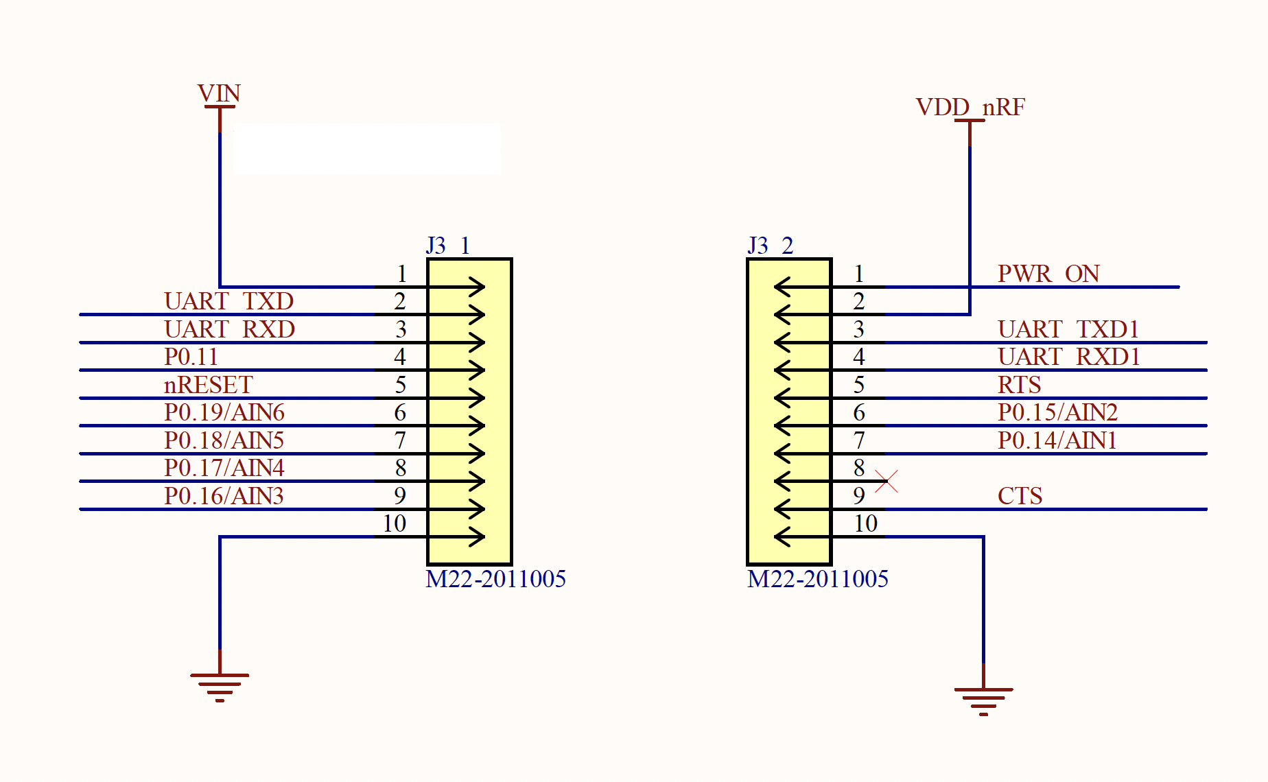
Following is an image showing the pinout of the socket.

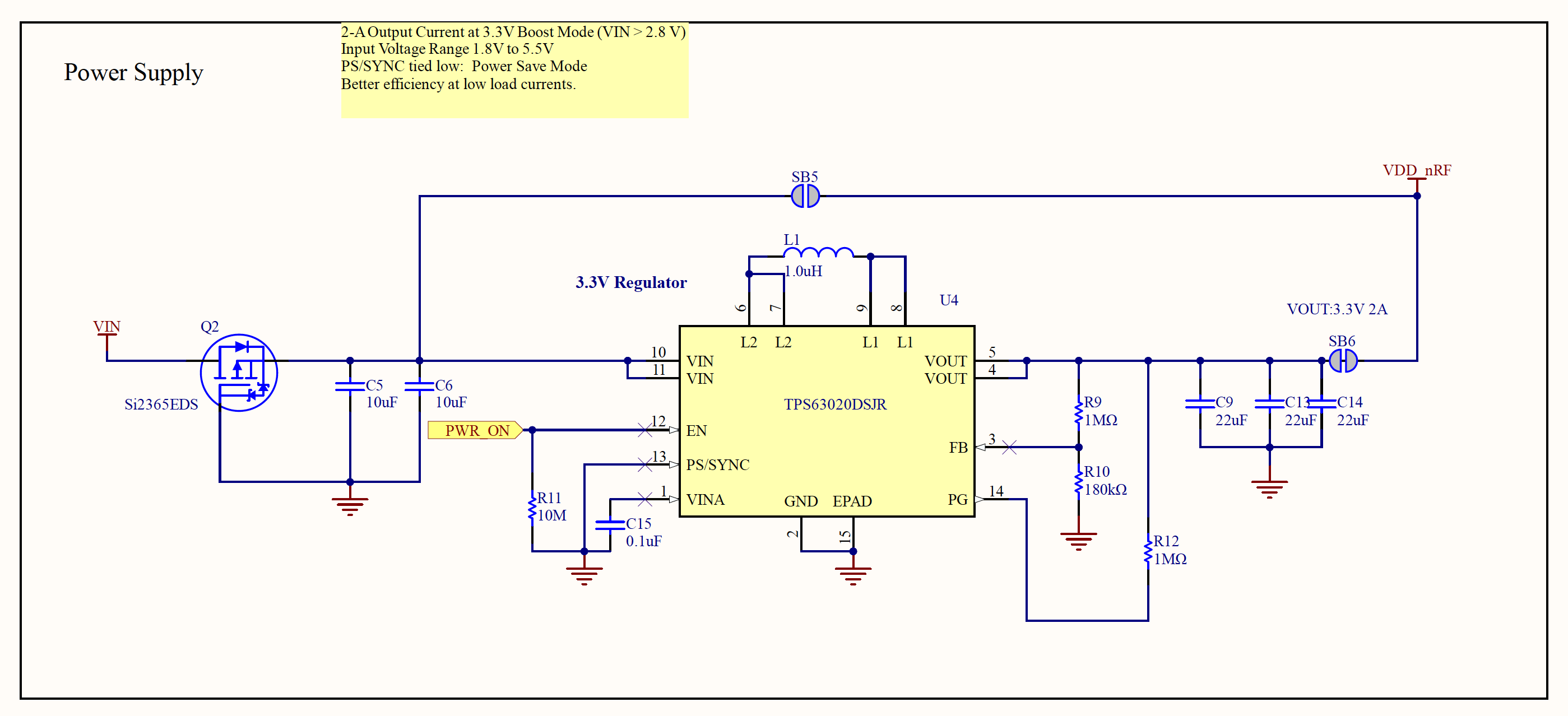
Following is an image of the onboard M1-N1 regulation.

J3_1-1 through J3_1-10 maps to other modules pins 1 through 10.
J3_2-1 through J3_2-10 maps to pins 20 through 11, where J3_2-1 is pin 20, J3_2-2 is pin 19, and so on to J3_2-10 being pin 11.
NOTE: ALL UART or GPIO pins operate at 3.3V and are connected to nRF9160 pins directly. These pins may be capable of operating at other voltages. Please consult the nRF9160 datasheet for details.
J3_1.1 - Pin 1 is power and although the M1-N1 supports 1.8V to 5.5V, if the user designs with 3.3V or 3.8V, then compatibility with other Signetik and non-Signetik modules can be achieved.
J3_1.2 - Pin 2 is UART TX (from M1-N1) and although it can be configured for other purposes, other modules lock this to UART TX
J3_1.3 - Pin 3 is UART RX (to M1-N1) and although it can be configured for other purposes, other modules lock this to UART RX
J3_1.4 - Pin 4 is a general GPIO pin but on competitor modules, this may be required to be GND. For maximum compatibility, a 0-ohm jumper to GND is ideal with the jumper DNP.
J3_1.5 - Pin 5 is a RESET input. It is best to control this from an MCU. For more details, see this article
J3_1.6 - Pin 6 is VUSB on some modules, but for the M1-N1 it is a GPIO pin. For maximum compatibility, it is suggested to not connect this pin at all.
J3_1.7 - Pin 7 is USB_P on some modules, but for the M1-N1 it is a GPIO pin. For maximum compatibility, it is suggested to not connect this pin at all.
J3_1.8 - Pin 8 is USB_N on some modules, but for the M1-N1 it is a GPIO pin. For maximum compatibility, it is suggested to not connect this pin at all.
J3_1.9 - Pin 9 is DTR on some modules and can be a GPIO or DTR on the M1-N1.
J3_1.10 - Pin 10 should be connected to GND
J3_2.1 - Pin 20 is ON_OFF for power enabling. Connect it to an MCU to drive it. Some modules will use this as a GPIO and so then it could be configured floating by the MCU.
J3_2.2 - Pin 19 is VDD regulated output (3.3V) on the M1-N1 but other modules use it as a GPIO or a RING signal. It is probably best to leave this connected for maximum compatibility OR use it to power your sensors and such, knowing that if you use another module you won't have this functionality.
J3_2.3 - Pin 18 is general GPIO or I2C at 1.8V on some modules. Can connect to an MCU as an input.
J3_2.4 - Pin 17 is general GPIO or I2C at 1.8V on some modules. Can connect to an MCU as an input.
J3_2.5 - Pin 16 is RTS or general GPIO
J3_2.6 - Pin 15 is a GPIO on the M1-N1 but some modules require it to be connected to GND. It is recommended to use a 0-ohm to GND and DNP it.
J3_2.7 - Pin 14 For the M1-N1, this is a GPIO but it may be VREF for ADCs on other modules. It is recommended to tie it to a voltage divider resistor network to achieve a good VREF but to leave these DNP for the M1-N1
J3_2.8 - Pin 13 has several functions across modules. It is best to connect to an MCU GPIO and tri-state it by default. Based on the module, you may need to drive this as an output or read as an input.
J3_2.9 - Pin 12 is CTS or a general GPIO on the M1-N1.
J3_2.10 - Pin 11 is GND on the M1-N1 and most modules, but some modules use this as a GPIO pin. Therefore, it is ideal to connect to GND through a 0-ohm jumper, which can be removed for modules that don't need this grounded.
Comments
5 comments
Thank you, Steve.
By the way, U.FL antenna connectors are placed on the bottom side of the M1-N1 module. So, I'm considering the M1-N1-LPC rather than the M1-N1-TC. Is this not good idea?
You are welcome! LPC is our preferred model as it is low profile and can easily be secured with PEMs and screws. We have the PEM studs available and if you use our dev kit reference design you can get the proper hole sizes for these studs.
See the 3rd link here for design files for the DEV-A1 PCB.
https://signetik.zendesk.com/hc/en-us/articles/1500011491722-Hardware-Information
Hi Steve,
I have a question for you. Does M1-N1 has a internal pull-up resistor on the reset input (pin J3_1.5)?
Thank you & happy Thanksgiving!
Steven
Hi Steve,
I have a question for you.
If I supply 4.0V to M1-N1 as its power, do I need a level shifter between M1-N1 and a micro-processor? The micro-processor is using 3.3V.
Thank you.
Steven
Please sign in to leave a comment.